This chapter will first analyze the various classes of instructions which should be available in a general-purpose computer. It will then analyze one by one all of the instructions available for the Z80, and explain in detail their purpose and the manner in which they affect flags or can be used in conjunction with various addressing modes. A detailed discussion of addressing techniques will be presented in Chapter 5.
Instructions may be classified in many ways, and there is no standard. We will distinguish five main categories of instructions:
Data transfer instructions will transfer data between registers, or between a register and memory, or between a register and an input/output device. Specialized transfer instructions may exist for registers which play a specific role. For example, push and pop operations are provided for efficient stack operation. They will move a word of data between the top of the stack and the accumulator in a single instruction, while automatically updating the stack pointer register.
Data processing instructions fall into five general categories:
It should be noted that, for efficient data processing, it is desirable to have powerful arithmetic instructions, such as multiply and divide. Unfortunately, they are not available on most microprocessors. It is also desirable to have powerful shift and skew instructions, such as shift n bits, or a nibble exchange, where the right half and the left half of the byte are exchanged. These are also usually unavailable on most microprocessors.
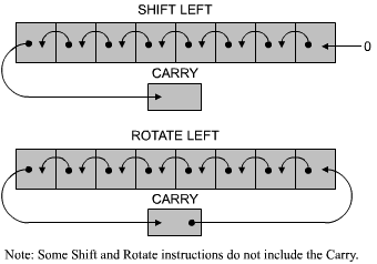
Before examining the actual Z80 instructions, let us recall the difference between a shift and a rotation. The shift will move the contents of a register or a memory location by one bit location to the left or to the right. The bit falling out of the register will go into the carry bit. The bit coming into the other side will be a "0" except in the case of an "arithmetic shift right," where the MSB will be duplicated.
In the case of a rotation, the bit coming out still goes into the carry. However, the bit coming in is the previous value which was in the carry bit. This corresponds to a 9-bit rotation. It is often desirable to have a true 8-bit rotation where the bit coming in on one side is the one falling from the other side. This is not provided on most microprocessors but is available on the Z80 (see Figure 4.1).
Finally, when shifting a word to the right, it is convenient to have one more type of shift, called a sign extension or an "arithmetic shift right." When doing operations on two's complement numbers, particularly when implementing floating-point routines, it is often necessary to shift a negative number to the right. When shifting a two's complement number to the right, the bit which must come in on the left side should be a "1" (the sign should get repeated as many times as needed by successive shifts). This is the arithmetic shift right.
Fig. 4.1: Shift and Rotate
The test instruction will test bits in the specified register for "0" or "1", or combinations. At a minimum, it must be possible to test the flags register. It is, therefore, desirable to have as many flags as possible in this register. In addition, it is convenient to be able to test for combinations of such bits with a single instruction. Finally, it is desirable to be able to test any bit position in any register, and to test the value of a register compared to the value of any other register (greater than, less than, equal). Microprocessor test instructions are usually limited to testing single bits of the flags register. The Z80, however, offers better facilities than most.
The jump instructions that may be available generally fall into three categories:
It is convenient to have two- or even three-way jumps, depending, for example, on whether the result of a comparison is "greater than," "less than," or "equal." It is also convenient to have skip operations, which will jump forward or backward by a few instructions. However, a "skip" is equivalent to a "jump." Finally, in most loops, there is usually a decrement or increment operation at the end, followed by a test-and-branch. The availability of a single-instruction increment/decrement plus test-and-branch is, therefore, a significant advantage for efficient loop implementation. This is not available in most microprocessors. Only simple branches, combined with simple tests, are available. This, naturally, complicates programming and reduces efficiency. In the case of the Z80, a "decrement and jump" instruction is available. However, it only tests a specific register (B) for zero.
Input/output instructions are specialized instructions for the handling of input/output devices. In practice, a majority of the 8-bit microprocessors use memory-mapped I/O: input/output devices are connected to the address bus just like memory chips, and addressed as such. They appear to the programmer as memory locations. All memory-type operations normally require 3 bytes and are, therefore, slow. For efficient input/output handling in such an environment, it is desirable to have a short addressing mechanism available so that I/O devices whose handling speed is crucial may reside in page 0. However, if page 0 addressing is available, it is usually used for RAM memory, which prevents its effective use for input/output devices. The Z80, like the 8080, is equipped with specialized I/O instructions. As a result, in the case of the Z80, the designer may use either method: input/output devices may be addressed as memory devices, or else as input/output devices, using the I/O instructions.
They will be described later in this chapter.
Control instructions supply synchronization signals and may suspend or interrupt a program. They can also function as a break or a similated interrupt. (Interrupts will be described in Chapter 6 on Input/Output Techniques.)
The Z80 microprocessor was designed to be a replacement for the 8080, and to offer additional capabilities. As a result of this design philosophy, the Z80 offers all the instructions of the 8080, plus additional instructions. In view of the limited number of bits available in an 8-bit opcode, one may wonder how the designers of the Z80 succeeded in implementing many additional ones. They did so by using a few unused 8080 opcodes and by adding an additional byte to the opcode for indexed operations. This is why some of the Z80 instructions occupy up to five bytes in the memory.
It is important to remember that any program can be written in many different ways. A thorough knowledge and understanding of the instruction set is indispensable for achieving efficient programming. However, when learning how to program, it is not essential to write optimized programs. During a first reading of this chapter, it is therefore unimportant to remember all the various instructions. It is important to remember the categories of instructions and to study typical examples. Then, when writing programs, the reader should consult the Z80 instruction set description, and select the instructions best suited to his needs. The various instructions of the Z80 will therefore be reviewed in logical categories. The reader interested in exploring the capabilities of the various instructions is referred to the individual descriptions of the instructions.
We will now examine the capabilities provided by the Z80 in terms of the five classes of instructions which have been defined at the beginning of this chapter.
Data transfer instructions on the Z80 may be classified in four categories: 8-bit transfers, 16-bit transfers, stack operations, and block transfers. Let us examine them.
All eight-bit data transfers are accomplished by load instructions. The format is:
LD destination, source
For example, the accumulator A may be loaded from register B by using the instruction:
LD A,B
Direct transfers may be accomplished between any two of the working registers (ABCDEHL).
In order to load any of the working registers, except for the accumulator, from a memory location, the address of this memory location must first be loaded into the H-L register pair.
For example, in order to load register C from memory location 1234, register H and L will first have to be loaded with the value "1234". (A load instruction operating on 16 bits will be used. This is described in the following section.)
Then, the instruction LD C,(HL) will be used and will accomplish the desired result.
The accumulator is an exception. It can be loaded directly from any specified memory location. This is called the extended addressing mode. For example, in order to load the accumulator with the contents of memory location 1234, the following instruction will be used:
LD A,(1234H) |
(Note the use of the "( )" to denote "contents of.") |
The instruction will be stored in the memory as follows:
| address | PC | : 3A | (opcode) |
| PC + 1 | : 34 | (low order half of the address) | |
| PC + 2 | : 12 | (high order half of the address) |
Note that the address is stored in "reverse order" in the instruction itself:
| 3A | low addr | high addr |
All the working registers may also be loaded with any specified eight-bit value, or "literal," contained in the second byte of the instruction (this is called immediate addressing). An example is:
LD E,12H
which loads register E with the value 12 hexadecimal.
In the memory, the instruction appears as:
| address | PC | : 1E | (opcode) |
| PC + 1 | : 12 | (literal operand) |
As a result of this instruction, the immediate operand, or literal value will be contained in register E.
The indexed addressing mode is also available for loading register contents, and will be fully described in the next chapter on addressing techniques. Other miscellaneous possibilities exist for loading specific registers, and a table listing all the possibilities is shown in Figure 4.2 (tables supplied by Zilog, Inc.). The grey areas show instructions common with the 8080A.
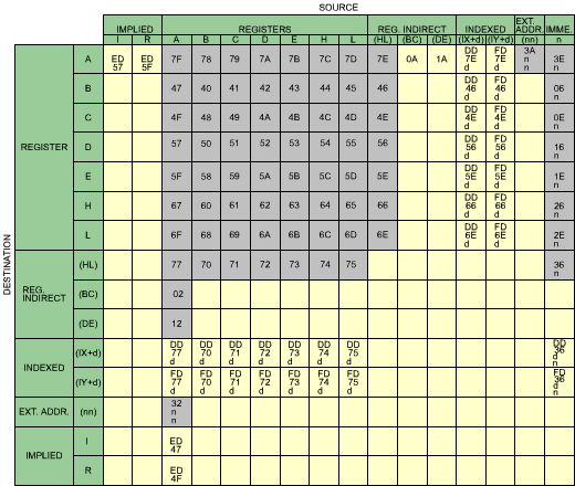
Fig. 4.2: Eight-Bit Load Group - 'LD'
Basically, any of the 16-bit register pairs, BC, DE, HL, SP, IX, IY, may be loaded with a literal 16-bit operand, or from a specified memory address (extended addressing), or from the top of the stack, i.e., from the address contained in SP. Conversely, the contents of these register pairs may be stored in the same manner at a specified memory address or on top of the stack. Additionally, the SP register may be loaded from HL, IX, and IY. This facilitates creating multiple stacks. The register pair AF may also be pushed on top of the stack.
The table listing all the possibilities is shown in Figure 4.3. The stack push and pop operations are included as parts of the 16-bit data transfers. All stack operations transfer the contents of a register pair to or from the stack. Note that there are no single push and pop instructions for saving individual eight-bit registers.
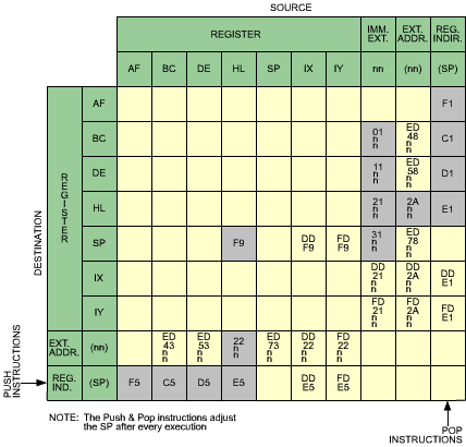
Fig. 4.3: 16-Bit Load Group - 'LD', 'PUSH' and 'POP'
A double-byte push or pop is always executed on a register pair: AF, BC, DE, HL, IX, IY (see the bottom row and the right-most column in Figure 4.3).
When operating on AF, BC, DE, HL, a single-byte is required for the instruction, resulting in good efficiency. For example, assume that the stack pointer SP contains the value "0100". The following instruction is executed:
PUSH AF
When pushing the contents of the register pair on the stack, the stack pointer SP is first decremented, then the contents of register A are deposited on top of the stack. Then the SP is decremented again, and the contents of F are deposited on the stack. At the end of the stack transfer, SP points to the top element of the stack, which in our example is the value of F.
It is important to remember that, in the case of the Z80, the SP points to the top of the stack and the SP is decremented whenever a register pair is pushed. Other conventions are often used in other processors, and this may be a source of confusion.
Additionally, a specialized mnemonic EX has been reserved for exchange operations. EX is not a simple data transfer, but a dual data transfer. It actually changes the contents of two specified locations. EX may be used to exchange the top of the stack with HL, IX, IY and also to swap the contents of DE and HL, and AF and AF' (remember that AF' stands for the other AF register pair available in the Z80).
Finally, a special EXX instruction is available to exchange the contents of BC, DE, HL with the contents of the corresponding registers in the second register bank of the Z80.
The possible exchanges are summarized in Figure 4.4.
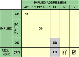
Fig. 4.4: Exchanges 'EX' and 'EXX'
Block transfer instructions are instructions which will result in the transfer of a block of data rather than a single or double byte. Block transfer instructions are more complex for the manufacturer to implement than most instructions and are usually not provided on microprocessors. They are convenient for programming, and may improve the performance of a program, especially during input/output operations. Their use and advantages will be demonstrated throughout this book. Some automatic block transfer instructions are available in the case of the Z80. They use specific conventions.
All block transfer instructions require te use of three pairs of registers: BC, DE, HL:
| BC is used as a 16-bit counter. This means that uup to 216 = 64K bytes may be moved automatically. HL is used as the source pointer. It may point anywhere in the memory. DE is used as the destination pointer and may point anywhere in the memory. |
Four block transfer instructions are provided:
LDD, LDDR, LDI, LDIR
All of them decrement the counter BC with each transfer. Two of them decrement the pointer registers DE and HL, LDD and LDDR, while the two others increment DE and HL, LDI and LDIR. For each of these two groups of instructions, the letter R at the end of the mnemonic indicates an automatic repeat. Let us examine these instructions.
LDI stands for "load and increment." It transfers one byte from the memory location pointed to by H and L to the destination in the memory pointed to by D and E. It also decrements BC. It will automatically increment H and L and D and E so that all register pairs are properly conditioned to perform the next byte transfer whenever required.
LDIR stands for "load, increment and repeat," i.e., execute LDI repeatedly until the counter registers BC reach the value "0". It is used to move a continuous block of data automatically from one memory area to another.
LDD and LDDR operate in the same way except that the address pointers are decremented rather than incremented. The transfer therefore starts at the highest address in the block instead of the lowest. The effect of the four instructions is summarized in Figure 4.5.
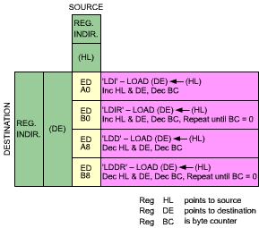
Fig. 4.5: Block Transfer Group
Similar automated instructions are available for CP (compare) and are summarized in Figure 4.6.
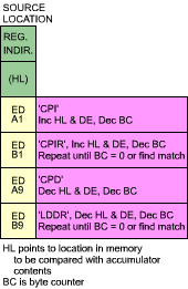
Fig. 4.6: Block Search Group
Two main arithmetic operations are provided: addition and subtraction. They have been used extensively in the previous chapter. There are two types of addition, with and without carry, ADC and ADD respectively. Similarly, two types of subtractions are provided, with and without carry. They are SBC and SUB.
Additionally, three special instructions are provided: DAA, CPL, and NEG. The Decimal Adjust Accumulator instruction DAA has been used to implement BCD operations. It is normally used for each BCD add or subtract. Two complementation instructions are available. CPL will compute the one's complement of the accumulator, and NEG will negate the accumulator into its complement format (two's complement).
All the previous instructions operate on eight-bit data. 16-bit operations are more restricted. ADD, ADC, and SBC are available on specific registers, as described in Figure 4.8.
Finally, increment and decrement instructions are available which operate on all registers, both in an eight-bit and a 16-bit format. They are listed in Figure 4.7 (eight-bit operations) and 4.8 (16-bit operations).
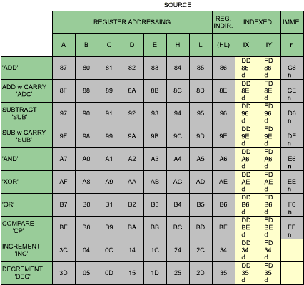
Fig. 4.7: Eight-Bit Arithmetic and Logic
Note that, in general, all artithmetic operations modify some of the flags. Their effect is fully described in the instruction descriptions later in this chapter. However, it is important to note that the INC and DEC instructions which operate on register pairs do not modify any of the flags. This detail is important to keep in mind. This means that if you increment or decrement one of the register pairs to the value "0", the Z-bit in the flags register F will not be set. The value of the register must be explicitly tested for the value "0" in the program.
Also, it is important to remember that the instructions ADC and SBC always affect all the flags. This does not mean that all the flags will necessarily be different after their execution. However, they might.
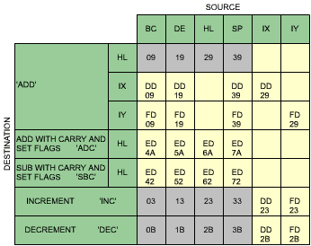
Fig. 4.8: Sixteen-Bit Arithmetic and Logic
Three logical operations are provided: AND, OR (inclusive) and XOR (exclusive), plus a comparison instruction CP. They all operate exclusively on eight-bit data. Let us examine them in turn. (A table listing all the possibilities and operation codes for these instructions is part of Figure 4.7.)
Each logical operation is characterized by a truth table, which expresses the logical value of the result in function of the inputs. The truth table for AND appears below:
| 0 AND 0 = 0 0 AND 1 = 0 1 AND 0 = 0 1 AND 1 = 1 |
or |
|
The AND operation is characterized by the fact that the output is "1" only if both inputs are "1". In other words, if one of the input is "0", it is guaranteed that the result is "0". This feature is used to zero a bit position in a word. This is called "masking."
One of the important uses of the AND instruction is to clear or "mask out" one or more specified bit positions in a word. Assume for example that we want to zero the right-most four-bit positions in a word. This will be performed by the following program:
LD   A,WORD          WORD CONTAINS '10101010'
AND  11110000B       '11110000' IS MASK
Let us assume that WORD is equal to '10101010'. The result of the program is to leave the value '10100000' in the accumulator. "B" is used to indicate a binary value.
| Exercise 4.1: | Write a three-line program which will zero bits 1 and 6 of WORD. |
| Exercise 4.2: | What happens with a MASK = '11111111'? |
This instruction is the inclusive OR operation. It is characterized by the following truth table:
| 0 OR 0 = 0 0 OR 1 = 1 1 OR 0 = 1 1 OR 1 = 1 |
or |
|
The logical OR is characterized by the fact that if one of the operands is "1", then the result is always "1". The obvious use of OR is to set any bit in a word to "1".
Let us set the right-most four bits of WORD to 1's. The program is:
LD   A,WORD
OR   00001111B
Let us assume that WORD did contain '10101010'. The final value of the accumulator will be '10101111'.
| Exercise 4.3: | What would happen if we were to use the instruction OR 10101111B? |
| Exercise 4.4: | What is the effect of ORing with "FF" hexadecimal? |
XOR stands for "exclusive OR." The exclusive OR differs from the inclusive OR that we have just described in one respect: the result is "1" only if one, and only one, of the operands is equal to "1". If both operands are equal to"1", the normal OR would give a "1" result. The exclusive OR gives a "0" result. The truth table is:
| 0 XOR 0 = 0 0 XOR 1 = 1 1 XOR 0 = 1 1 XOR 1 = 0 |
or |
|
The exclusive OR is used for comparisons. If any bit is different, the exclusive OR of two words will be non-zero. In addition, in the case of the Z80, the exclusive OR may be used to complement a word, since there is no complement instruction on anything but the accumulator. This is done by performing the XOR of a word with all ones. The program appears below:
LD   A,WORD
XOR  11111111B
Let us assume the WORD contained "10101010". The final value of the register will be "01010101". You can verify that it is the complement of the original value.
XOR can be used to advantage as a "bit toggle."
| Exercise 4.5: | What is the effect of XOR using a register with "00" hexadecimal? |
Let us first differentiate between the shift and the rotate operations, which are illustrated in Figure 4.9. In a shift operation, the contents of the register are shifted to the left or to the right by one bit position. The bit which falls out of the register goes into the carry bit C, and the bit which comes in is zero. This was explained in the previous section.
Fig. 4.9: Shift and Rotate
One exception exists: it is the shift-right-arithmetic. When performing operations on negative numbers in the two's complement format, the left-most bit is the sign bit. In the case of negative numbers it is "1". When dividing a negative number by "2" by shifting it to the right, it should remain negative, i.e., the left-most bit should remain "1". This is performed automatically by the SRA instruction or Shift Right Arithmetic. In this arithmetic shift right, the bit which comes in on the left is identical to the sign bit. It is "0" if the left-most bit was a "0", and "1" if the left-most bit was a "1". This is illustrated on the right of Figure 4.10, which shows all the possible shift and rotate operations.
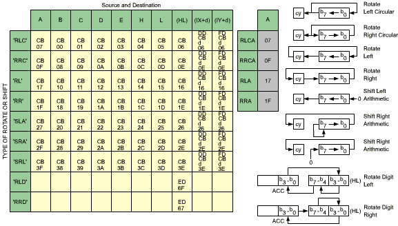
Fig. 4.10: Rotates and Shifts
A rotation differs from a shift by the fact that the bit coming into the register is the one which will fall from either the other end of the register or the carry bit. Two types of rotations are supplied in the case of the Z80: an eight-bit rotation and a nine-bit rotation.
The nine-bit rotation is illustrated in Figure 4.11. For example, in the case of a right rotation, the eight bits of the register are shifted right by one bit position. The bit which falls off the right part of the register goes, as usual, into the carry bit. At the same time the bit which comes in on the left end of the register is the previous value of the carry bit (before it is overwritten with the bit falling out). In mathematics this is called a nine-bit rotation since the eight bits of the register plus the ninth (the carry bit) are rotated to the right by one bit position. Conversely, the left rotation accomplishes the same result in the opposite direction.
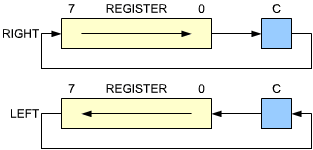
Fig. 4.11: Nine-Bit Rotation
The eight-bit rotation operate in a similar way. Bit 0 is copied into bit seven, or else bit seven is copied into bit 0, depending on the direction of the rotation. In addition, the bit coming out of the register is also copied in the carry bit. This is illustrated by Figure 4.12.
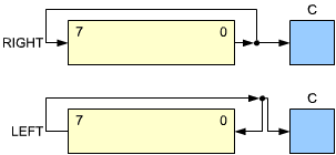
Fig. 4.12: Eight-Bit Rotation
Two special digit-rotate instructions are provided to facilitate BCD arithmetic. The result is a four-bit rotation between two digits contained in the memory location pointed to by the HL registers and the digit in the lower half of the accumulator. This is illustrated by Figure 4.13.

Fig. 4.13: Digit Rotate Instruction (Rotate Decimal)
It has been shown above how the logical operations may be used to set or reset bits or groups of bits in the accumulator. However, it is convenient to set or reset any bit in any register or memory location with a single instruction. This facility requires a considerable number of opcode and is therefore usually not provided on most microprocessors. However, the Z80 is equipped with extensive bit-manipulation facilities. They are shown in Figure 4.14. This table also includes the test instructions which will be described only in the next section.
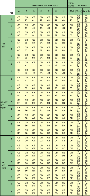
Fig. 4.14: Bit Manipulation Group
Two special instructions are also available for operating on the carry flag. They are CCF (Complement Carry Flag) and SCF (Set Carry Flag). They are shown in Figure 4.15.
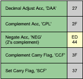
Fig. 4.15: General-Purpose AF Operations
Since testing operations rely heavily on the use of the flags register, we will here describe in detail the role of each of the flags. The contents of the flags register appear in Figure 4.16.
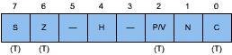
Fig. 4.16: The Flags Register
C is the carry, N is add or subtract, P/V is parity or overflag, H is half carry, Z is zero, S is sign. Bits 3 and 5 of the flags register are not used ("-"). The two flags H and N are used for BCD arithmetic and cannot be tested. The other four flags (C, P/V, Z, S) can be tested in conjunction with conditional jump or call instructions.
The role of each flag will now be described.
In the case of nearly all microprocessors, and of the Z80 in particular, the carry bit assumes a double role. First, it is used to indicate whether an addition or subtraction operation has resulted in a carry (or borrow). Secondly, it is used as a ninth bit in the case of shift and rotate operations. Using a single bit to perform both roles facilitates some operations, such as a multiplication operation. This should be clear from the explanation of the multiplication which has been presented in the previous chapter.
When learning to use the carry bit, it is important to remember that all arithmetic operations will either set or reset it, depending on the result of the instructions. Similarly, all shift and rotate operations use the carry bit and will either set it or reset it, depending on the value of the bit which comes out of the register.
In the case of logical instructions (AND, OR, XOR), the carry bit will always be reset. They may be used to zero the carry explicitly.
Instructions which affect the carry bit are:
This flag is normally not used by the programmer, and is used by the Z80 itself during BCD operations. The reader will remember from the previous chapter that, following a BCD add or subtract, a DAA (Decimal Adjust Accumulator) instruction is executed to obtain the valid BCD results. However, the "adjustment" operation is different after an addition and after a subtraction. The DAA therefore executes differently, depending on the value of the N flag. The N flag is set to "0" after an addition and is set to a "1" after a subtraction.
The symbol used for this flag, "N", may be confusing to programmers who have used other processors, since it may be mistaken for the sign bit. It is an internal operation sign bit.
N is set to "0" by:
N is set to "1" by:
The parity/overflow flag performs two different functions. Specific instructions will set or reset this flag depending on the parity of the result; parity is determined by counting the total number of ones in the result. If this number is odd, the parity bit will be set to "0" (odd parity). If it is even, the parity bit will be set to "1" (even parity). Parity is most frequently used on blocks of characters (usually in the ASCII format). The parity bit is an additional bit which is added to the seven-bit code representing the character, in order to verify the integrity of data which has been stored in a memory device. For example, if one bit in the code representing the character has been changed by accident, due to a malfunction in the memory device (such as a disk or RAM memory), or during transmission, then the total number of ones in the seven-bit code will have been changed. By checking the parity bit, the discrepancy will be detected, and an error will be flagged. In particular, the flag is used with logical and rotate instructions. Also, naturally, during an input operation from an I/O device, the parity flag will indicate the parity of the data being read.
For the reader familiar with the Intel 8080, note that the parity flag in the 8080 is used exclusively as such. In the case of the Z80, it is used for several additional functions. This flag should therefore be handled with care when going from one of the microprocessors to the other.
In the case of the Z80, the second essential use of this flag is as an overflow flag (not available in the 8080). The overflow flag has been described in Chapter 1, when the two's complement notation was introduced. It detects the fact that, during an addition or subtraction, the sign of the result is "accicentally" changed due to the overflow of the result into the sign bit. (Recall that, using an eight-bit representation, the largest positive number is +127, and the smallest negative number is -128 in two's complement.)
Finally, this bit is also used, in the case of the Z80, for two unrelated functions.
During the block transfer instructions (LDD, LDDR, LDI, LDIR), and during the search instructions (CPD, CPDR, CPI, CPIR), this flag is used to detect whether the counter register B has attained the value "0". With decrementing instructions, this flag is reset to"0" if the byte counter register pair is "0". When decrementing, it is reset if BC-1 = 0 at the beginning of the instruction, i.e., if BC will be decremented to "0" by the instruction.
Finally, when executing the two special instructions LD A,I and LD A,R, the P/V flag reflects the value of the interrupt enable flip-flop (IFF2). This feature can be used to preserve or test this value.
The P flag is affected by:
The V flag is affected by:
It is also used by:
The half-carry flag indicates a possible carry from bit 3 into bit 4 during an arithmetic operation. In other words, it represents the carry from the low order nibble (group of 4 bits) into the high order one. Clearly, it is primarily used for BCD operations. In particular, it is used internally within the microprocessor by the Decimal Adjust Accumulator (DAA) instruction in order to adjust the result to its correct value.
This flag will be set during an addition when there is a carry from bit 3 to bit 4 and reset when there is no carry. Conversely, during a subtract operation, it will be set if there is a borrow from bit 4 to bit 3, and reset if there is no borrow.
The flag will be conditioned by addition, subtraction, increment, decrement, comparisons, and logical operations.
Instructions which affect the H bit are:
Note that the H bit is randomly affected by the 16-bit add and subtract instructions, and by block input and output instructions.
The Z flag is used to indicate whether the value of a byte which has been computed, or is being transferred, is zero. It is also used with comparison instructions to indicated a match, and for other miscellaneous functions.
In the case of an operation resulting in a zero result, or of a data transfer, the Z bit is set to "1" whenever the byte is zero. Z is reset to "0" otherwise.
In the case of comparison instructions, the Z bit is set to "1" whenever the comparison succeeds and to "0" otherwise.
Additionally, in the case of the Z80, it is used for three more functions: it is used with the BIT instruction to indicated the value of a bit being tested. It is set to "1" if the specified bit is "0" and reset otherwise.
With the special "block input-output instructions" (INI, IND, OUT, OUTD), the Z flag is set if D - 1 = 0, and reset otherwise; it is set if the byte counter will decrement to "0" (INIR, INDR, OTIR, OTDR).
Finally, with the special instructions IN r,(C), the Z flag is set to "1" to indicate that the input byte has the value "0".
In summary, the following instructions condition the value of the Z bit:
Usual instructions which do not affect the Z bit are:
This flag reflects the value of the most significant bit of a result or a byte being transferred (bit seven). In two's complement notation, the most significant bit is used to represent the sign. "0" indicates a positive number and a "1" indicates a negative number. As a result, bit seven is called the sign bit.
In the case of most microprocessors, the sign bit plays an important role when communicating with input/output devices. Most microprocessors are not equipped with a BIT instruction for testing the contents of any bits in a register or the memory. As a result, the sign bit is usually the most convenient bit to test. When examining the status of an input/output device, reading the status register will automatically condition the sign bit, which will be set to the value of bit seven of the status register. It can then be tested conveniently by the program. This is why the status register of most input/output chips connected to microprocessor systems have their most important indicator (usually ready/not ready) in bit position seven.
A special BIT instruction is provided in the case of the Z80. However, in order to test a memory location (which may be the address of an I/O status register), the address must first be loaded into register IX, IY or HL. There is no bit instruction provided to test a specific memory address directly (i.e., no direct addressing mode for this instruction). The value of positioning an input/output ready flag in bit position seven, therefore, remains intact, even in the case of the Z80.
Finally, the sign flag is used by the special instruction IN r,(C) to indicate the sign of the data being read.
Instructions which affect the sign bit are:
The flag bits are used to automatically detect special conditions within the ALU of the microprocessor. They can be conveniently tested by specialized instructions, so that specific action can be taken in response to the condition detected. It is important to understand the role of the various indicators available, since most decisions taken within the program will be taken in function of these flag bits. All jumps executed within a program will jump to the specified locations depending on the status of these flags. The only exception involves the interrupt mechanism, which will be described in the chapter on input/output and may cause jumping to specific locations whenever a hardware signal is received on specialized pins of the Z80.
At this point, it is only necessary to remember the main function of each of these bits. When programming, the reader can refer to the description of the instruction later in this chapter to verify the effect of every instruction on the various flags. Most flags can be ignored most of the time, and the reader who is not yet familiar with them should not feel intimidated by their apparent complexity. Their use will become clearer as we examine more application programs.
A summary of the six flags and the way they are set or reset by the various instructions is shown in Figure 4.17.
| INSTRUCTION | C | Z | P/V | S | N | H | COMMENTS |
|---|---|---|---|---|---|---|---|
| AND A,s; ADC A,s | | | | | V | | | 0 | | | 8-bit add or add with carry |
| SUB s; SBC A,s; CP s; NEG | | | | | V | | | 1 | | | 8-bit subtract, subtract with carry, compare and negate accumulator |
| AND s | 0 | | | P | | | 0 | 1 | Logical operations |
| OR s; XOR s | 0 | | | P | | | 0 | 0 | And sets different flags |
| INC r | | | V | | | 0 | | | 8-bit increment | |
| DEC m | | | V | | | 1 | | | 8-bit decrement | |
| ADD DD,ss | | | 0 | X | 16-bit add | |||
| ADC HL,ss | | | | | V | | | 0 | X | 16-bit add with carry |
| SBC HL,ss | | | | | V | | | 1 | X | 16-bit subtract with carry |
| RLA; RLCA; RRA; RRCA | | | 0 | 0 | Rotate accumulator | |||
| RL m; RLC m; RR m; RRC m; SLA m; SRA m; SRL m | | | | | P | | | 0 | 0 | Rotate and shift location m |
| RLD; RRD | | | P | | | 0 | 0 | Rotate digit left and right | |
| DAA | | | | | P | | | | | Decimal adjust accumulator | |
| CPL | 1 | 1 | Complement accumulator | ||||
| SCF | 1 | 0 | 0 | Set carry | |||
| CCF | | | 0 | X | Complement carry | |||
| IN r,(C) | | | P | | | 0 | 0 | Input register indirect | |
| INI; IND; OUTI; OUTD | | | X | X | 1 | X | Block input and output Z=0 if B |
|
| INIR; INDR; OTIR; OTDR | 1 | X | X | 1 | X | ||
| LDI; LDD | X | | | X | 0 | 0 | Block transfer instructions P/V=1 if BC |
|
| LDIR; LDDR | X | 0 | X | 0 | 0 | ||
| CPI; CPIR; CPD; CPDR | | | | | | | 1 | X | Block search instructions Z=1 if A = (HL), otherwise Z=0 P/V=1 if BC |
|
| LD A,I; LD A,R | | | IFF | | | 0 | 0 | The contents of the interrupt enable flip-flop (IFF) is copied into the P/V flag | |
| BIT b,s | | | X | X | 0 | 1 | The complement of bit b of location s is copied into the Z flag |
The following notation is used in this table:
| SYMBOL | OPERATION |
|---|---|
| C | Carry/link flag. C=1 if the operation produced a carry from the MSB of the operand or result. |
| Z | Zero flag. Z=1 if the result of the operation is zero. |
| S | Sign flag. S=1 if the MSB of the result is one. |
| P/V | Parity or overflow flag. Parity (P) and overflow (V) share the same flag. Logical operations affect this flag with the parity of the result while arithmetic operations affect the overflow of the result. If P/V holds parity, P/V=1 if the result of the operation is even, PV=0 if the result is odd. If P/V holds overflow, P/V=1 if the result of the operation produced an overflow. |
| H | Half-carry flag. H=1 if the add or subtract operation produced a carry into or borrow from bit 4 of the accumulator. |
| N | Add/Subtract flag. N=1 if the previous operation was a subtract. H and N flags are used in conjunction with the decimal adjust instruction (DAA) to properly correct the result into packed BCD format following addition or subtraction using operands with packed BCD format. |
| | | The flag is affected according to the result of the operation. |
| The flag is unchanged by the operation. | |
| 0 | The flag is reset by the operation. |
| 1 | The flag is set by the operation. |
| X | The flag is a "don't care." |
| V | The P/V flag is affected according to the overflow result of the operation. |
| P | The P/V flag is affected according to the parity result of the operation. |
| r | Any of the CPU registers A, B, C, D, E, H, L. |
| s | Any 8-bit location for all the addressing modes allowed for the particular instruction. |
| ss | Any 16-bit location for all the addressing modes allowed for that instruction. |
| ii | Any one of the two index register IX or IY. |
| R | Refresh counter. |
| n | 8-bit value in range <0..255>. |
| nn | 16-bit value in range <0..65535>. |
| m | Any 8-bit location for all the addressing modes allowed for the particular instruction. |
Fig. 4.17: Summary of Flag Operation
A branch instruction is an instruction which causes a forced branching to a specified program address. It changes the normal flow of execution of the program from a sequential mode into one where a different segment of the program is suddenly executed. Jumps may be conditional or unconditional. An unconditional jump is one in which the branching occurs to a specific address, regardless of any other condition.
A conditional jump is one which occurs to a specific address only if one or more conditions are met. This is the type of jump instruction used to make decisions based upon data or computed results.
In order to explain the conditional jump instructions, it is necessary to understand the role of the flags register, since all branching decisions are based upon these flags. This was the purpose of the preceding section. We can now examine in more detail the jump instructions provided by the Z80.
Two main types of jump instructions are provided: jump instructions within the main program (they are called "jumps"), and the special type of branch instructions used to jump to a subroutine and to return from it ("call" and "return"). As a result of any jump instruction, the program counter PC will be reloaded with a new address, and the usual program execution will resume from this point on. The full power of the various jump instructions can be understood only in the context of the various addressing modes provided by the microprocessor. This part of the discussion will be deferred until the next chapter, where the addressing modes are discussed. We will only consider here the other aspects of these instructions.
Jumps may be unconditional (branching to a specified memory address) or else conditional. In the case of a conditional jump, one of four flag bits may be tested. They are the Z, C, P/V, and S flags. Each of them may be tested for the value "0" or "1".
The corresponding abbreviations are:
In addition, a special combination instruction is available in the Z80 which will decrement the B register and jump to a specified memory address as long as it is not zero. This is a powerful instruction used the terminate a loop, and it has already been used several times in the previous chapter: it is the DJNZ instruction.
Similarly, the CALL and the RET (return) instructions may be conditional or unconditional. They test the same flags as the branch instruction which we have already described.
The availability of conditional branches is a powerful resource in a computer and is generally not provided on other eight-bit microprocessors. It improves the efficiency of programs by implementing in a single instruction what requires two instructions otherwise.
Finally, two special return instructions have been provided in the case of interrupt routines. They are RETI and RETN. They will be described in the section of Chapter 6 on interrupts.
The addressing modes and the opcodes for the various branches available are shown in Figure 4.18.
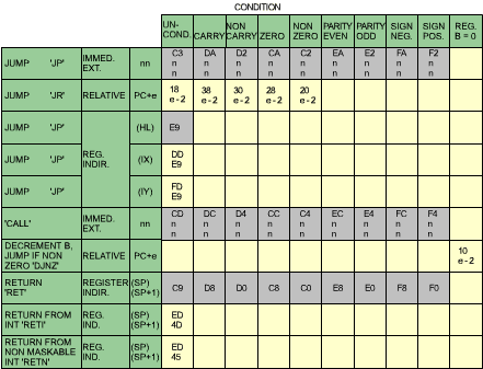
Fig. 4.18: Jump Instructions
A detailed discussion of the various addressing modes is presented in Chapter 5.
By examining Figure 4.18, it becomes apparent that many addressing modes are restricted. For example, the absolute jump JP nn can test four flags, while JR can only test two flags.
Note another observation: JR tends to be used whenever possible as it is shorter than JP (one less byte) and facilitates program relocation. However, JR and JP are not interchangeable: JR cannot test the parity or the sign flags.
One more type of specialized branch is available; the is the restart or RST instruction. It is a one-byte instruction which allows jumping to any one of eight starting addresses at the low end of the memory. Its starting addresses are, in decimal, 0, 8, 16, 24, 32, 40, 48 and 56. It is a powerful instruction because it is implemented in a single byte. It provides a fast branch, and for this reason is used essentially to respond to interrupts. However, it is also available to the programmer for other uses. A summary of the opcodes for this instruction is shown in Figure 4.19.
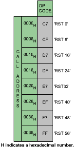
Fig. 4.19: Restart Group
Input/output techniques will be described in detail in Chapter 6. Simply, input/output devices may be addressed in two ways: as memory locations, using any of the instructions that have already been described, or using specific input/output instructions. Usual memory addressing instructions use three bytes: one byte for the opcode and two bytes for the address. As a result, they are slow to execute, since they require three memory accesses. The main purpose of specialized input/output instructions is to provide shorter and, therefore, faster instructions. However, input/output instructions have two disadvantages.
First, they "waste" several of the precious few opcodes available (since usually only 8 bits are used to supply all the opcodes necessary for a microprocessor). Secondly, they require the generation of one or more specialized input/output signals, and therefore "waste" one or more of the few pins available in the microprocessor. The number of pins is usually limited to 40. Because of these possible disadvantages, specific input/output instructions are not provided in most microprocessors. They are, however, provided on the original 8080 (the first powerful eight-bit general-purpose microprocessor introduced) and on the Z80, which we know is compatible with the 8080.
The advantage of input/output instructions is to execute faster by requiring only two bytes. However, a similar result can be obtained by supplying a special addressing mode called "page 0" addressing, where the address is limited to a field of eight bits. This solution is often chosen in other microprocessors.
The two basic input/output instructions are IN and OUT. They transfer either the contents of the specified I/O locations into any of the working registers or the contents of the register into the I/O device. They are naturally two bytes long. The first byte is reserved for the opcode, the second byte of the instructions forms the low part of the address. The accumulator is used to supply the upper part of the address. It is therefore possible to select one of the 64K devices. However, this requires that the accumulator be loaded with the appropriate contents every time, and this may slow the execution.
Additionally, the Z80 provides a register-indirect mode, plus four specialized block-transfer instructions for input and output.
In the register-input mode, whose format is IN r,(C), the register pair B and C is used as a pointer to the I/O device. The contents of B are placed on the high order part of the address bus. The contents of the specified I/O device are then loaded into the register designated by r.
The same applies to the OUT instruction.
The four block-transfer instructions on input are: INI, INIR (repeated INI), IND and INDR (repeate IND). Similarly, on output, they are OUTI, OTIR, OUTD, and OTDR.
In this automated block transfer, the register pair H and L is used as a destination pointer. Register C is used as the I/O device selector (one out of 256 devices). In the case of the output instruction, H and L point to the source. Register B is used as a counter and can be incremented or decremented. The corresponding instructions on input are INI when incrementing and IND when decrementing.
INI is an automated single-byte transfer. Register C selects the input device. A byte is read from the device and is transferred to the memory address pointed to by H and L. H and L are then incremented by 1,and the counter B is decremented by 1.
INIR is the same instructions, automated. It is executed repeatedly until the counter decrements to "0". Thus, up to 256 bytes may be transferred automatically. Note that to achieve a total transfer of exactly 256, register B should be set to the value "0" prior to executing this instruction.
The opcodes for the input and output instructions are summarized in Figures 4.20 and 4.21.
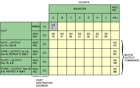
Fig. 4.20: Output Group
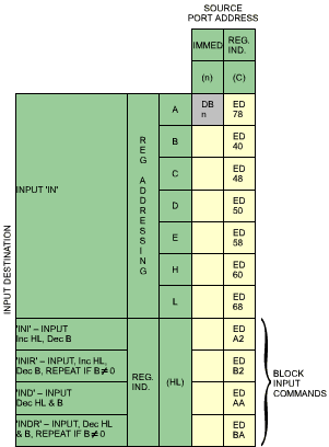
Fig. 4.21: Input Group
Control instructions are instructions which modify the operating mode of the CPU or manipulate its internal status information. Seven such instructions are provided.
The NOP instruction is a no-operation instruction which does nothing for one cycle. It is typically used either to introduce a deliberate delay (4 states = 2 microseconds with a 2 MHz clock), or to fill the gaps created in a program during the debugging phase. In order to facilitate program debugging, the opcode for the NOP is traditionally all 0's. This is because, at execution time, the memory is often cleared, i.e., all 0's. Executing NOP's is guaranteed to cause no damage and will not stop the program execution.
The HALT instruction is used in conjunction with interrupts or a reset. It actually suspends the operation of the CPU. The CPU will then resume operation whenever either an interrupt or a reset signal is received. In this mode, the CPU keeps executing NOP's. A halt is often placed at the end of programs during debugging phase, as there is usually nothing else to be done by the main program. The program must then be explicitly restarted.
Two specialized instructions are used to disable and enable the internal interrupt flag. They are EI and DI. Interrupts will be described in Chapter 6. The interrupt flag is used to authorize or not authorize the interruption of a program. To prevent interrupts from occurring during any specific portion of a program, the interrupt flip-flop (flag) may be disabled by this instruction. It will be used in Chapter 6. These instructions are shown in Figure 4.22.
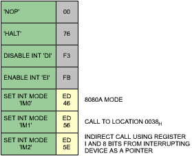
Fig. 4.22: Miscellaneous CPU Control
Finally, three interrupt modes are provided in the Z80. (Only one is available on the 8080). Interrupt mode 0 is the 8080 mode, interrupt mode 1 is a call to location 038H, and interrupt mode 2 is an indirect call which uses the contents of teh special register I, plus 8 bits provided by the interrupting device as a pointer to the memory locations whose contents are the address of the interrupt routine. These modes will be explained in Chapter 6.
Two types of interrupts may reach the Z80. They are the IRQ and the NMI pins. They will also be explained in Chapter 6.
The five categories of instructions available on the Z80 have now been described. The details on individual instructions are supplied in the following section of the book. It is not necessary to understand the role of each instruction in order to start to program. The knowledge of a few essential instructions of each type is sufficient at the beginning. However, as you begin to write programs by yourself, you should learn about all the instructions of the Z80 if you want to write good programs. Naturally, at the beginning, efficiency is not important, and this is why most instructions can be ignored.
One important aspect has not yet been described. This is the set of addressing techniques implemented on the Z80 to facilitate the retrieval of data within the memory space. These addressing techniques will be studied in the next chapter.